Turning Ideas into Silicon Reality

At the forefront of semiconductor innovation, we provide end-to-end silicon design services ranging from chip architecture to physical design to tape-out.
Whether you’re building advanced compute platforms or specialized ASICs, we will accelerate your path to silicon success.
Services
System Architecture & RTL Development
A premium product begins with carefully engineered SoC architecture and microarchitecture, designed for scalability, performance, and efficient data movement. These foundational decisions define product capability and serve as key differentiators in competitive markets.
Our experienced team develops high-quality, synthesizable RTL using proven design methodologies to achieve optimal performance, area, and power efficiency. When performance demands extend beyond digital logic, we apply our analog expertise to deliver enhanced system performance and superior product differentiation.

Integration, Verification & Validation
Comprehensive verification and validation ensure functional correctness across all levels of abstraction, from block-level to an integrated system, reducing risk before silicon. Detailed IP integration ensures cohesive system operation and consistent performance across interfaces and hierarchies.
FPGA prototyping and software co-validation extend verification to the next level, enabling real-time system simulations and early bring-up of real-world use cases. This approach reduces risk, minimizes costly re-spins, and accelerates time to market. Our dedicated software team supports parallel development to ensure hardware and software readiness from the start.
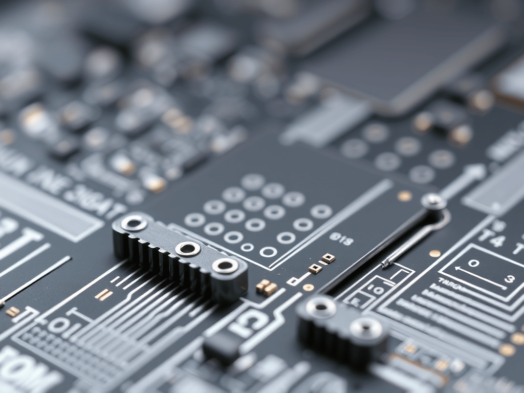
Physical Design & Layout
From floorplan to final GDSII, our physical design team transforms verified RTL into layouts optimized for performance, power, and reliability. The process includes floorplanning, place-and-route (PnR), and full-custom layout for analog and mixed-signal components.
Rigorous physical verification (DRC/LVS) ensures compliance with foundry design rules, while post-layout timing and signal-integrity analysis confirm design closure across all operating conditions. Every transistor is optimized for maximum efficiency, ensuring silicon area is utilized to its fullest potential.
Power, Performance & Test
Power and performance optimization are driven by detailed analysis and disciplined implementation. Back-annotated results are examined thoroughly to identify opportunities for power reduction and timing improvement across all design stages. Design-for-Test (DFT) methodologies are integrated early to maximize coverage and enable efficient production testing.
This focused approach delivers predictable silicon behavior, faster bring-up, and higher yield, ensuring each design meets its performance and reliability targets.
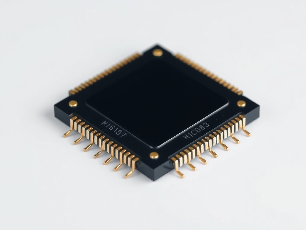
Manufacturing & Silicon Operations
Our silicon operations team manages the final stages of chip realization. From tape-out management and foundry coordination to wafer logistics and packaging and assembly, we handle the complexities of production with precision.
Leveraging strategic foundry relations, we ensure a smooth path to silicon. Comprehensive test planning and validation complete the cycle, delivering production-ready devices with security and confidence. The result is a smooth path to high-volume manufacturing, supported by proven scalability and reliable execution.

Leadership

Jim Seto, CEO
Jim is a semiconductor industry veteran with over 30 years of experience in chip development, global operations, and supply chain leadership.
He played a key role in the growth of ATI contributing to its $5.4B acquisition by AMD. He served as Vice President of Foundry Developments and Advisor at AMD, and Vice President of Supply Chain, Operations & Procurement.
At Qualcomm, Jim was Vice President of Operations and M&A Integration Planning, where he oversaw the supply of 6 billion chips annually and led major engineering and operational transformation initiatives.
With deep experience from initial design through mass production, Jim brings trusted, industry-tested leadership to EPIC ASIC.

Earl Mai, CTO
Earl brings over 25 years of ASIC design experience, having held senior engineering roles at leading global semiconductor companies, including Senior Member of Technical Staff at AMD and Member of Technical Staff at ON Semiconductor.
At AMD, he led engineering teams developing custom shader architectures for the PlayStation 4 and PlayStation 5, consoles that have shipped more than 140 million units worldwide. Recognized as a world-class ASIC architect, Earl has delivered multiple chip designs across diverse applications and possesses expertise spanning the full design spectrum—from transistor-level implementation to system-level integration.
As CTO, Earl provides engineering-driven leadership grounded in deep, end-to-end silicon architecture expertise.
Why Choose Us?

Full Cycle Expertise
Our experienced team brings deep expertise across the entire breadth of chip development, ranging from architecture exploration to new product introduction. This end-to-end perspective allows us to anticipate challenges, apply insights, and deliver innovative solutions.
Driven by Performance & Efficiency
With extensive experience in high-performance compute (HPC) designs, we understand the challenges of moving large amounts of data at speed while maintaining power efficiency. Our deep insight into system architecture, network topologies, and power optimization enables us to deliver silicon that achieves exceptional PPA (Performance, Power, and Area) across demanding compute workloads.
Advanced Technology Process Collaboration
We maintain strong working relationshiaps and direct access to leading-edge foundries such as TSMC, enabling us to stay aligned with process roadmap changes, design rules, and sign-off requirements. This visibility ensures our customers benefit from the latest process optimizations, predictable tape-out schedules, and first-time-right silicon at advanced nodes.
Implementation Highlights
High-Performance Compute SoC
End-to-end execution from architecture to tape-out and NPI
High-Bandwidth Data Movement Design
Memory-bound design for large data transfers with high throughput and low latency
Power Optimization and Custom Analog Integration
Back-annotated power analysis and custom analog macros to achieve measurable power savings
Custom CPU Architecture
Bespoke ISA and optimized pipeline to meet specialized compute requirements
Hardware Infrastructure for AI Datacenter
4×1 PCIe interface board with hot-pluggable PSU for scalable AI infrastructure